Parallel Synthesis Technologies
Silicon Microfabrication Techniques
Bulk Micromachining:
Bulk Micromachining is the process of sculpting features in bulk of materials such as silicon, quartz, etc. by treatment with either orientation dependent (anisotropic) or by orientation independent (isotropic) etchants. It is widely used to fabricate membranes, beams, holes and grooves and other features. In silicon micromachining, the bulk micromachining starts with a single crystal silicon substrate (usually a (100) oriented wafer) on which a thin film of material that is inert to chemical etchants (etch stop) is deposited. The film is then selectively patterned photolithographically to allow the removal of undesired portions of the etch stop film. The bulk material is then etched using either wet chemical etching or dry etching, or both, depending on the requirements.
i. Wet Etching (KOH Etching):
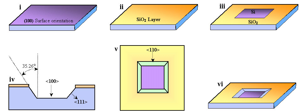
Wet etching a (100) oriented Si wafer with KOH etches rectangular pits into the surface with the bottom of the well formed from the (100) plane and the sides from four <111> planes. The fabrication starts (i) with a silicon wafer which is (ii) oxidized in steam to form a dense, thick (0.5 µ) coating of SiO2. Patterning the surface photolithographically (iii) and selective removal of the oxide exposes a bare Si surface which is etched with hot KOH to yield the aforementioned rectangular pits (views parallel, perpendicular and obliquely, to the plane of the wafer in iv, v and vi, respectively).
Wet Etching of (100) Silicon Wafer
ii. Deep Reactive Ion Etching (DRIE):
Dry Etching techniques (Plasma etching) are used for etching features with variable tapering and high aspect ratio microstructures. The most common forms of dry etching for micromachining applications are isotropic ion etching and anisotropic deep reactive ion etching (DRIE). Deep channels and pits (up to few tens of microns deep) with nearly vertical walls and of arbitrary shape can be etched. Unlike anisotropic wet etching, DRIE etching is not controlled by the relative etch rates of the silicon crystal planes.Surface Micromachining
Silicon surface micromachining uses the same equipment and processes as the electronics semiconductor industry. This technique deposits layers of sacrificial and structural material on the surface of a silicon wafer. As each layer is deposited it is patterned, leaving material only where the designer wishes. When the sacrificial material is removed, completely formed and assembled mechanical devices are left.
Photolithography
The process of transferring a pattern from a photomask on to the Silicon wafer is called photolithography. Silicon wafer is oxidized in steam to form a dense, thick (0.5 µ) layer of SiO2, followed by coating a thin layer of photoresist. Portions of the photoresist are then exposed to UV radiation through photomask (quartz plate) with a pattern. Exposed photoresist is rendered soluble and removed with a developer solution. The photoresist pattern is used as a mask to etch the exposed SiO2 layer. The SiO2 pattern is then used to etch and sculpt the silicon with either wet or dry etching.Bonding
Bonding of two substrates or micromachined silicon wafers is desired in certain processes to form complex devices and structures (such as valves, pumps, etc). By applying heat, high electric field or pressure or a combination of the above to two materials, a hermetic, high-strength bond can be obtained.
Types of bonding:
· Fusion bonding (Si - Si)
· Anodic bonding (Si - Glass) and
· Adhesive, Eutetic, etc.Dicing
Dicing procedures involve slicing/cutting silicon wafers with microprocessor controlled high speed diamond saws. Depending upon the material and requirement, kerf may be as small as 20 µ, and dies may be diced as small as .01" (250 µ).Packaging
The packaging of the micro structures or devices meets the following requirements:
· Enable the user to handle the device easily
· Protects the device in harsh environments
· Prevents it from mechanical damage, chemical attack, or high temperatures